Engineering High-Speed Board-to-Board Connector Interfaces for Multigigabit Data Transmission and Signal Integrity Optimization
Learn the critical design principles behind high speed board to board connector selection, focusing on pin density, stack heights, and cross-vendor intermateable compatibility.
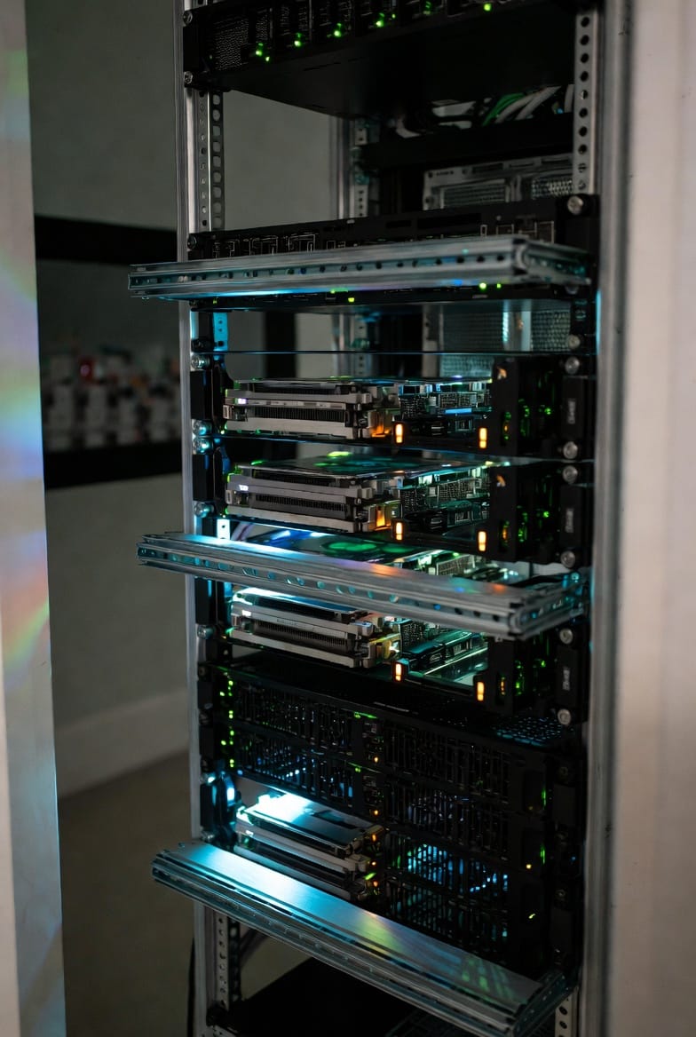
As electronic devices shrink in physical footprint while scaling exponentially in data processing capabilities, the internal architecture of PCBs must adapt. Traditional wired interconnects inside devices are rapidly being replaced by dense, multi-board stacked configurations. At the heart of this design philosophy is the high speed board to board connector, a highly engineered component optimized to pass multi-gigabit data streams between coplanar, perpendicular, or parallel circuit boards. Achieving seamless transmission at frequencies exceeding 28 GHz requires an intimate understanding of contact geometries, impedance matching, and industry standards.
Standard board-to-board choices are typically designed for low-frequency control signals or power routing, prioritizing cost and basic mechanical durability. In contrast, a high-speed variation is an entirely different class of hardware. Every element of its internal physical architecture is precision-modeled to act as a continuous transmission line. Key differentiating features include: Integral Ground Planes—high-speed configurations feature built-in metallic ground plates situated between rows of signal pins, providing low-impedance return paths and eliminating crosstalk between adjacent differential signal pairs. Hermaphroditic or Low-Profile Contacts—advanced contact structures minimize the physical length of the electrical path, reducing propagation delay and parasitic capacitance. Variable Stack Heights—manufacturers offer parallel mezzanine connectors in various stack heights without sacrificing high-frequency electrical performance.
In electronic sourcing and design, the concept of being intermateable is critical. A connector is considered intermateable if it can physically mate with, and function perfectly alongside, a connector manufactured by a competing vendor. In the high-speed ecosystem, true cross-vendor compatibility can be difficult to guarantee due to proprietary pin shapes, localized patent designs, and tight manufacturing tolerances. However, industry standards like PCIe, Open Compute Project (OCP), and COM Express mandate specific open architectures. When selecting a high-speed connector interface, engineers must verify whether a secondary source component is fully intermateable in terms of footprint, wipe length, spatial clearance, and signal integrity performance. Utilizing verified intermateable components protects the manufacturing supply chain from single-source component bottlenecks.
Implementing high-speed interconnects requires strict adherence to advanced layout techniques on the surrounding PCB. When a differential trace moves from the horizontal plane of a PCB into the vertical plane of a connector, it encounters physical discontinuities. To maintain an uncompromised signal path, designers must optimize the footprint breakout region. This involves configuring precise anti-pads (clearances in the copper ground planes directly beneath the connector pins) to minimize capacitive coupling. Furthermore, the vias used to route signals from internal PCB layers to the connector pads must be backdrilled to eliminate unused copper stubs, which would otherwise act as resonant antennas and distort the high-frequency waveforms.
By combining precision-engineered connector hardware with meticulous PCB layout practices, system architects can achieve flawless data rates across complex, multi-board embedded systems, clearing the path for the next generation of computing performance.