Overcoming the 112G and 224G Signal Wall in Next-Gen Data Centers
As data centers transition to 112 Gbps and 224 Gbps per lane, traditional copper traces are hitting physical limits. Inside the high-speed connector revolution.
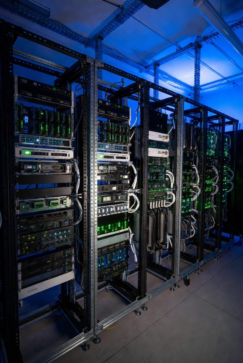
Data centers are the engine rooms of the digital economy, and their performance is governed by how fast they can route bits across a circuit board. With the rise of AI cluster scaling, the industry is transitioning rapidly from 112 Gbps PAM4 signaling to 224 Gbps PAM4 per lane. At these extreme frequencies, electrical signals behave less like currents flowing through copper and more like high-frequency radio waves.
The Death of the Standard PCB Trace
At 224 Gbps, routing high-speed lines directly through standard PCB glass-epoxy laminates (like FR4) introduces unacceptable insertion loss and signal distortion.
To solve this, hardware designers are turning to Cabled Backplane Architecture. Instead of routing signals through the motherboard, high-speed cables plug directly into connectors sitting immediately adjacent to the ASIC (Application-Specific Integrated Circuit).
Traditional Routing:
[ ASIC ] ─── (Lossy PCB Copper Trace) ─── [ Backplane Connector ]
Cabled Bypass Routing:
[ ASIC ] ─── [ Near-Chip Connector ] === (Low-Loss Twinax Cable) === [ Backplane ]
By bypassing the PCB entirely via ultra-low-loss twinaxial cables, engineers can preserve signal integrity across the server chassis, keeping error rates well within acceptable limits without needing hot, power-hungry active signal amplifiers.